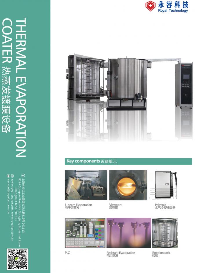
What is Cathodic Arc Depositon?
Cathodic arc deposition or Arc-PVD is a physical vapor deposition technique in which an electric arc is used to vaporize material from a cathode target. The vaporized material then condenses on a substrate, forming a thin film. The technique can be used to deposit metallic, ceramic, and composite films.
Cathodic arc depositon process:
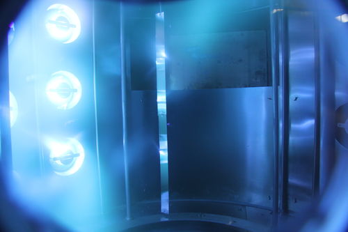
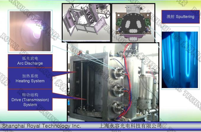
The arc evaporation process begins with the striking of a high current, low voltage arc on the surface of a cathode (known as the target) that gives rise to a small (usually a few micrometres wide), highly energetic emitting area known as a cathode spot. The localised temperature at the cathode spot is extremely high (around 15000 °C), which results in a high velocity (10 km/s) jet of vapourised cathode material, leaving a crater behind on the cathode surface. The cathode spot is only active for a short period of time, then it self-extinguishes and re-ignites in a new area close to the previous crater. This behaviour causes the apparent motion of the arc.
As the arc is basically a current carrying conductor it can be influenced by the application of an electromagnetic field, which in practice is used to rapidly move the arc over the entire surface of the target, so that the total surface is eroded over time.
The arc has an extremely high power density resulting in a high level of ionization (30-100%), multiple charged ions, neutral particles, clusters and macro-particles (droplets). If a reactive gas is introduced during the evaporation process, dissociation, ionization and excitation can occur during interaction with the ion flux and a compound film will be deposited.
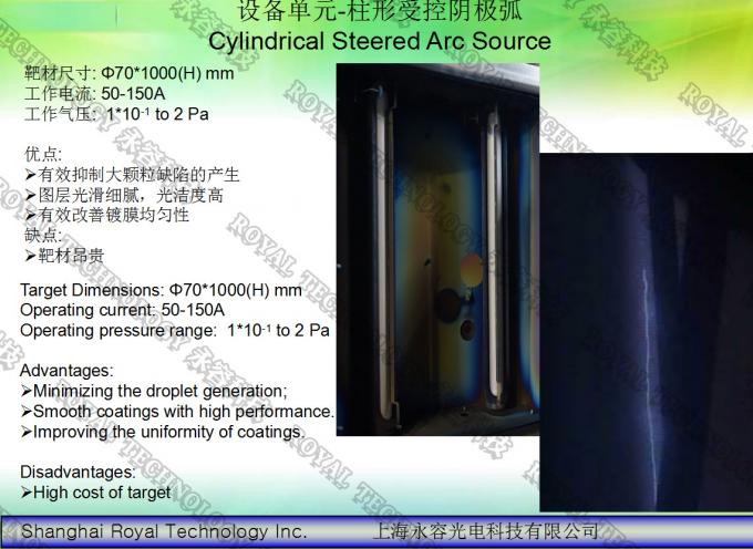
One downside of the arc evaporation process is that if the cathode spot stays at an evaporative point for too long it can eject a large amount of macro-particles or droplets. These droplets are detrimental to the performance of the coating as they are poorly adhered and can extend through the coating. Worse still if the cathode target material has a low melting point such as aluminium the cathode spot can evaporate through the target resulting in either the target backing plate material being evaporated or cooling water entering the chamber. Therefore, magnetic fields as mentioned previously are used to control the motion of the arc. If cylindrical cathodes are used the cathodes can also be rotated during deposition. By not allowing the cathode spot to remain in one position too long aluminium targets can be used and the number of droplets is reduced. Some companies also use filtered arcs that use magnetic fields to separate the droplets from the coating flux.
Cathodic Arc Deposition Application:
Cathodic arc deposition is actively used to synthesize extremely hard film to protect the surface of cutting tools and extend their life significantly. A wide variety of thin hard-film, Superhard coatings and nanocomposite coatings can be synthesized by this technology including TiN, TiAlN, CrN, ZrN, AlCrTiN and TiAlSiN.
This is also used quite extensively particularly for carbon ion deposition to create diamond-like carbon films. Because the ions are blasted from the surface ballistically, it is common for not only single atoms, but larger clusters of atoms to be ejected. Thus, this kind of system requires a filter to remove atom clusters from the beam before deposition. The DLC film from filtered-arc contains extremely high percentage of sp3diamond which is known as tetrahedral amorphous carbon, or ta-C.
Filtered Cathodic arc can be used as metal ion/plasma source for Ion implantation and Plasma Immersion Ion Implantation and Deposition (PIII&D).
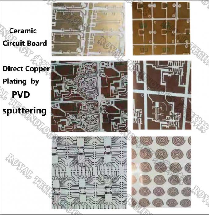
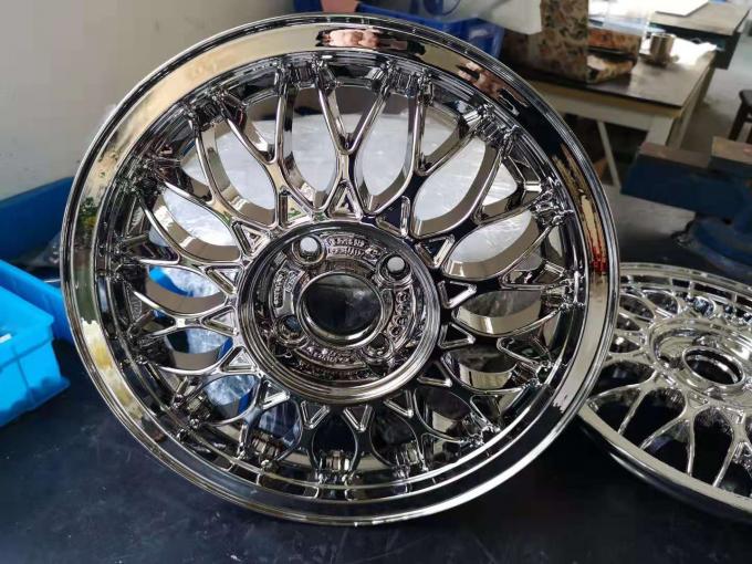
The round cathodic arc cathodes and cylindrical arc cathode are widely used for various PVD decorative coatings.

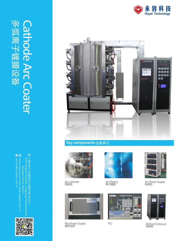
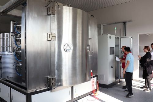
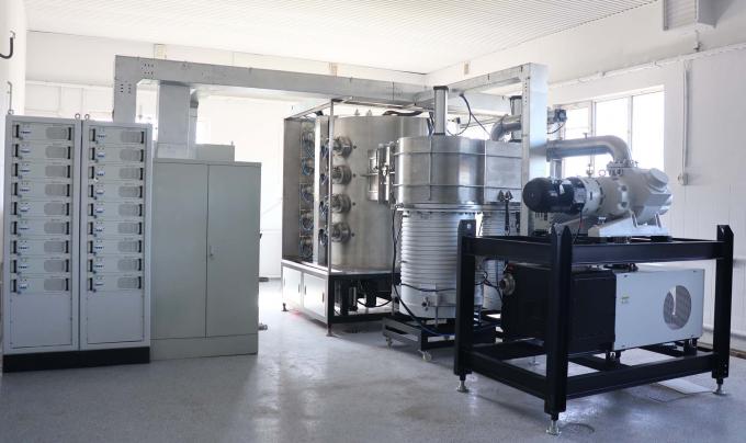
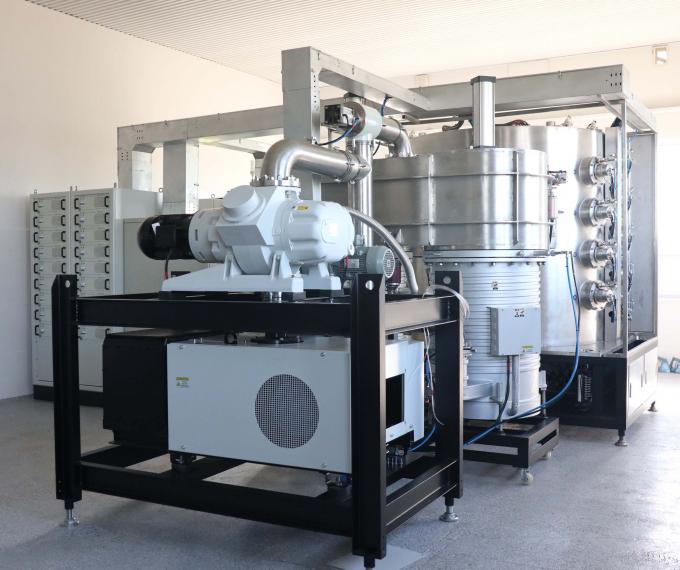
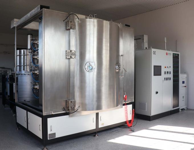
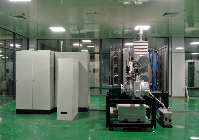
Multi Arc Vacuum Coater’s Design:
Sablev type Cathodic arc source, which is the most widely used in the West, consists of a short cylindrical shape electrical conductive target at cathode with one open end. This target has an electrically-floating metal ring surrounded working as an arc confinement ring (Strel’nitskij shield). The anode for the system can be either the vacuum chamber wall or a discrete anode. Arc spots are generated by mechanical trigger (or igniter) striking on open end of the target making a temporarily short circuit between the cathode and anode. After the arc spots being generated they can be steered by magnetic field or move randomly in absence of magnetic field.
Aksenov Quarter-torus duct macroparticle filter using plasma optical principles which was developed by A. I. Morozov
The plasma beam from Cathodic Arc source contains some larger clusters of atoms or molecules (so called macro-particles), which prevent it from being useful for some applications without some kind of filtering. There are many designs for macro-particle filters and the most studied design is based on the work by I. I. Aksenov et al. in 70’s. It consists of a quarter-torus duct bent at 90 degrees from the arc source and the plasma is guided out of the duct by principle of plasma optics.
There are also other interesting designs such as a design which incorporates a straight duct filter built-in with truncated cone shape cathode as reported by D. A. Karpov in the 90’s. This design became quite popular among both the thin hard-film coaters and researchers in Russia and former USSR countries until now. Cathodic arc source can be made into the long tubular shape (extended-arc) or long rectangular shape but both designs are less popular.
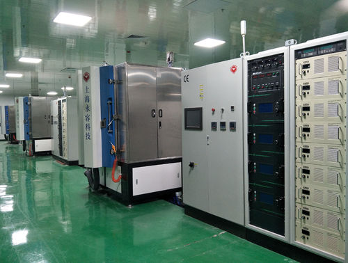
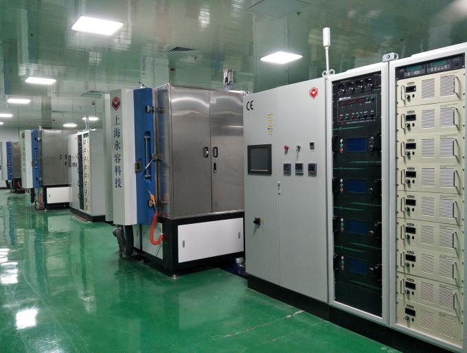
Please consult Royal Technology for your demand and applications. Our team is honored to serve you with our passion and technique.