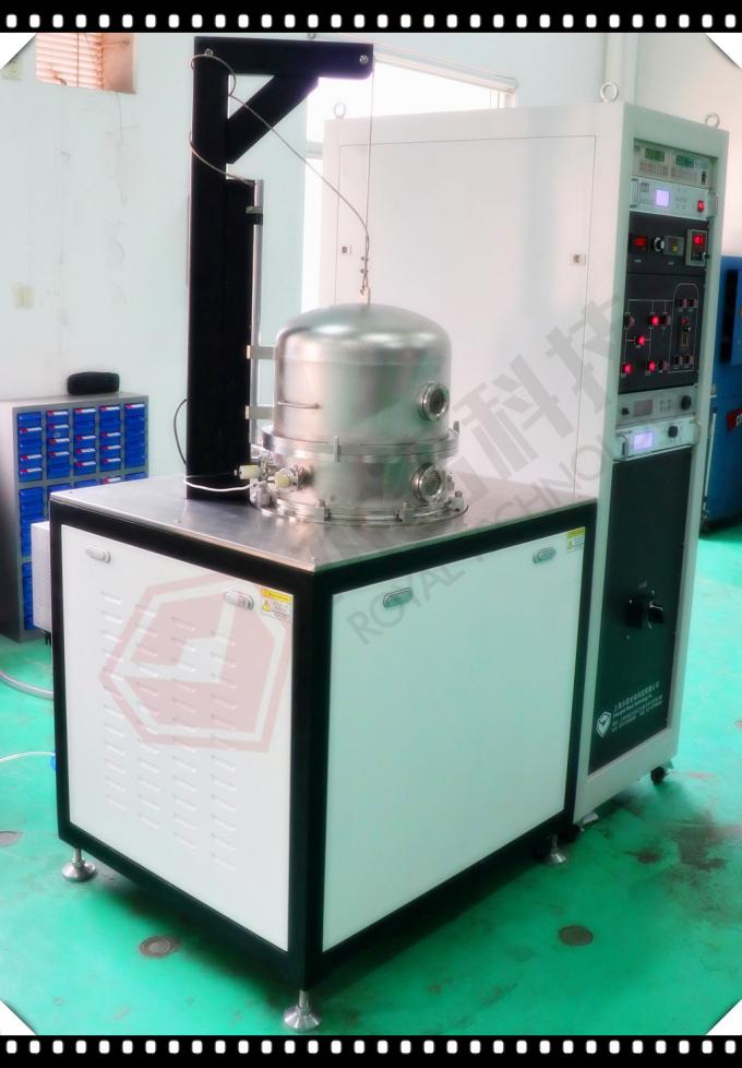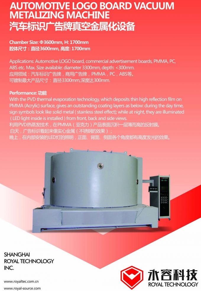
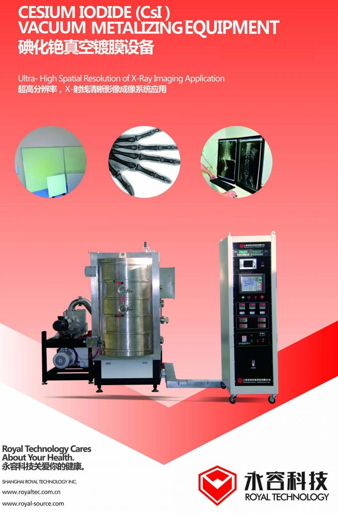
Automotive LOGO Board Vacuum Metallizing Machine
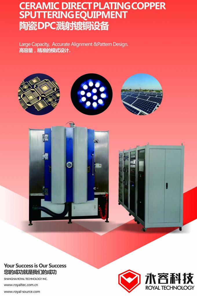
The DPC process- Direct Plating Copper is an advanced coating technology applied with LED / semiconductor / electronic industries. One typical application is Ceramic Radiating Substrate. Cooper conductive film deposition on Aluminum Oxide (Al2O3), AlN substrates by PVD vacuum sputtering technology, compared with traditional manufacturing methods: DBC LTCC HTCC, much lower production cost is its top feature.
Royal technology team assisted our customer to develope the DPC process successfully with PVD sputtering technology.
Keywords: Ceramic sealing parts, DPC process, Copper PVD Sputtering system, LED Ceramic Chips With Cooper Plating, Al2O3, AlN Ceramic Circuit Boards, Al2O3 Plates On LED, Semiconductor
Applications of DPC:
· HBLED
· Substrates for solar concentrator cells
· Power semiconductor packaging including automotive motor control
· Hybrid and electric automobile power management electronics
· Packages for RF
· Microwave devices
DPC Technology Performance
Various substrate materials: Ceramic (Al3O2, AlN), Glass, and Si
Nowadays, in view of global technology industry, it’s quite important for all manufacturers to develop and find the best coating solutions to improve products quality and lowering production cost, plus, have to take care of our environment.
Especially in automotive industry, as an essential transportation tool of human being, it is an indispensable part of our daily life. So how to solve “energy shortage – petrol”
“ Petrol burning emitting CO2 and hazardeous gas out, bringing pollution to our planet” “ high production costs” issues. Thanks to PVD coating technology, which has solved these problems and improving this bad situation.
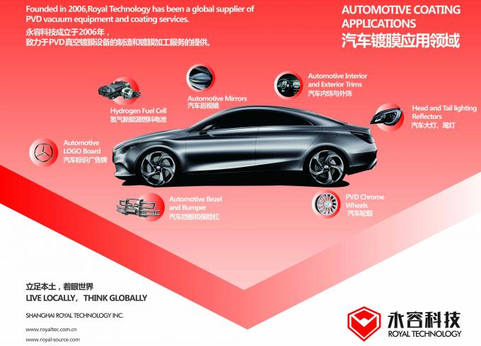
PVD technology has been widely used in various parts of vehicle manufacturing process, please review below image and learn what Royal Tec can provide for you:
1. Vacuum Metallizing Equipment
A: Automotive Lighting Reflectors
B: Exterior & Interior Trims, handles
C: Automotive LOGO LED board
D: Bezels and bumpers
2. PVD Hard Chrome Sputtering System
A: Car Wheels
B: Car Mirrors
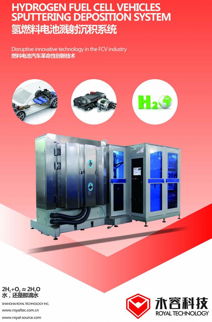
3. Hydrogen Fuel Cell Sputtering System in the FCV industry with PECVD + PVD Technology
FCV is the short name of Fuel Cell Vehicles, it is the newest technology for next generation of green cars. It is different from the primary battery such as dry cell and rechargeable battery that needs to repeat charging, and is 100% environmentally friendly.
The core technology is about generating the electrical energy with fuel cell power module through electrochemical reaction between hydrogen as fuel and oxygen. Scientists, engineers, professors from transportation organizations and worldwide vehicles manufactures have made thousands tests and finally developed the proper process.
Royal Technology has been working closely with customers in the past 3 years and has successfully designed and fabricated the high efficiency, commercialized and standardized sputtering deposition system. We believe this technology will be absolutely disruptive change in the vehicles industry.
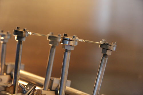
The RTSP1213 machine is a batch model sputtering system, can deposit various hard coatings, soft coatings, compound films and solid lubricating films on the metallic and non-metallic materials substrates. Applied to industries of Hydrogen Fuel Cell vehicles, photonic products, aerospace and other new energy industries.
Properties:
To improve the conductivity of surface;
High corrosion resistance;
High wear resistance;
High hardness
Hydrophobic composition film and other functional films
Available for compound coatings: metallic and non-metallic films.
Film thickness range from 100nm to 12μm, thickness tolerance ±5%
Strong adhesion.
Low tempering parts surface hardening treatment.
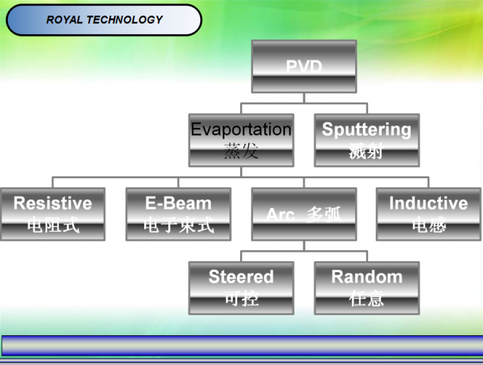
General Information About PVD Process
PVD processes is atomic deposition process in which material vaporized from a source is transported in the form of a vapor through a vacuum or low-pressure gaseous or plasma environment to the substrate, where it condenses. PVD processes can be used to deposit films of elements and molecules and also of compound materials by the reaction of depositing material with the ambient gas environment. ( e.g., TiN ) or with a co-depositing material (e.g. TiC ). Typically, PVD processes are used to deposit films with thickness in the range of a few nanometers to thousands of nanometers; however, they can be used to form graded-composition deposits of multi-layer coatings, very thick deposits, and freestanding structures.
Royal Technology aims to improve our standard of living with advanced environmentally friendly coating solutions.
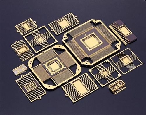
Direct Plated Copper Metallized Substrate and Its Application on Microwave Circuits
A direct plated copper (DPC) metallized substrate technique is introduced and characterized in this article. The proposed DPC metallized substrate provides the main advantages of excellent thermal management and high-frequency characteristics, due to t…
The direct plated copper (DPC) process on metallized ceramic substrate was originally created to replace the direct bonded copper (DBC) process because of its better electrical, thermal and mechanical performance.1 Compared to DBC, DPC provides a very strong bond strength between the Al2O3/AlN substrate and the copper metal, due to the use of a thin film bonding layer.2 DPC also has a good ability in thickness control for the copper layer, from very thin to very thick. For fine pitch design, a minimum conductor line width/spacing of 3 mils can be easily obtained, and via holes are filled with copper for good electrical and thermal characteristics. By using the proposed DPC substrate, superior performance can be obtained compared to other technologies in terms of its features and applications, which includes high circuit density, outstanding high-frequency characteristics, excellent thermal management and heat-transfer performance, outstanding solderability, and wire-bonding assembly characteristics. These DPC substrates can therefore be widely used for high frequency components that require high power and high heat.
In this article, the DPC fabrication is briefly described with a process flow chart, to introduce several key attributes of this process. A simple electrical characterization for DPC substrate is then utilized to extract the high-frequency dielectric constant and dissipation factor. Finally, a 10 GHz, parallel-coupled line bandpass filter is designed to validate the extracted dielectric parameters and the excellent high-frequency performance of a DPC metallized substrate.
Direct Plated Copper Process
The entire DPC process basically comprises the steps displayed in Figure 1, which include defining holes in the ceramic substrate, sputtering a copper film onto the ceramic substrate, forming a dry film onto the copper film, forming a circuit diagram with exposure and development, plating copper leads, removing the dry film and etching the seed metal copper.3 The detailed processes have been described by S.P. Ru,4 with more theoretical explanations and drawings.
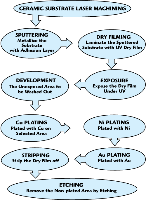
Figure 1 DPC process flow chart.
With the flow chart shown, the DPC process is started by defining holes on the bare ceramic substrate with a laser. These holes can be used as via holes to communicate between both sides of the ceramic substrate if it is necessary for some specific designed layout. Then a copper film, used as a seed metal layer, is sputtered on the opposite sides of the ceramic substrate so that it is covered with a copper layer. From the artwork describing the circuit diagram, a photomask is made using conventional photomask technology. The photomask is flatly positioned and adheres to the dry film on the ceramic substrate, which is sent into an exposing chamber.
After creating a vacuum in the exposing chamber, ultraviolet rays irradiate the dry film through the photomask, which is polymerized by the ultraviolet radiation. The dry film, which is not irradiated by the ultraviolet rays, does not react and keeps its chemical composition. The development process etches the polymerized part of the dry film by chemical cleaning or physical cleaning. In this way, some parts of the copper film are exposed from the dry film; those parts of the copper film will form the required circuit diagram as per the artwork of the circuit, in order to produce the required copper areas of a circuit on the ceramic substrate. Thus, the circuit layout can be printed on the dry film.
Copper is then deposited to fill the exposed parts of the dry film on the ceramic substrate, with suitable conductor thickness and width, by a plating technology to form the copper circuit. By the above processes, the metallized circuit area has slender, flat and smooth characteristics, and the heat dissipation is good. Then nickel and gold are deposited on the upper surface of the copper. The nickel film prevents the atoms of the copper leads diffusing into the gold film. The gold film avoids the oxidization of the conductor surface and improves the adhesion for the gold bonding wires. An optical resistance is formed on the upper surface of the copper. The remaining dry film on the ceramic substrate is then removed. After stripping the dry film, the copper circuit is protected by the nickel and gold films. The detaching copper film process etches the copper film not protected by the optical resist.
Due to the processes described and the materials used, several key attributes of the DPC process can be summarized as below:
· Superior thermal performance
· Low electrical resistance conductor lines
· Stable up to temperature > 340°C
· Accurate feature location, compatible with automated, large format assembly
· Fine line resolution allowing high density of devices and circuitry
· Proven reliability
· Mechanically rugged ceramic construction
· Low cost, high performance ceramic solution
The applications of DPC metallized substrate can be selected on high-brightness LED (HBLED), substrates for solar concentrator cells, power semiconductor packaging and automotive motor control. In addition, DPC substrates with excellent electrical performance can be considered for RF/microwave components, which require very low loss.
Electrical Properties Extraction
In order to utilize DPC substrates for RF/microwave applications, the dielectric properties must be extracted. Dielectric characterization is a very important issue for electronic packaging designs since electrical behavior is greatly influenced by the dielectric constant and dielectric loss at high frequencies.
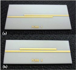
Figure 2 DPC microstrip parallel-coupled resonators with distinct output connections: (a) PCMR1 and (b) PCMR4.
There are numerous reported methods in the published literature.5-8 Many of these methods have one or several limitations, such as expensive and complicated instrumentation, difficult-to-fabricate fixtures, measured dielectric properties only valid for one particular frequency, poor repeatability, and inability to obtain both dielectric constant and dielectric loss. However, in this article, a simple approach is used to obtain the accurate dielectric factors for further substrate design and simulation.
Holzman used a computer model of the resonator to extract the dielectric data.9 Once the circuit is modeled accurately with a computer-aided design (CAD) simulator, the substrate’s dielectric properties can be determined by comparing the predictions from the simulator with the measured characteristics. This empirical/analytical approach has been demonstrated by a number of researchers in the microwave field.

Figure 3 Measured and simulated results for the microstrip parallel-coupled resonators: (a) PCMR1 and (b) PCMR4.
Therefore, to extract high-frequency dielectric data for DPC substrate, two modified microstrip parallel-coupled resonators with distinct zeros over a broad bandwidth were fabricated.Figure 2shows the photos of parallel-coupled microstrip resonators (PCMR). The PCMR1 shown affects transmission zeros with more depth at lower frequencies; PCMR4 generates transmission zeros with deeper depth at higher frequencies. The two resonators have the same coupled-line structure with a line distance of 570 mils and a spacing of 12 mils, but opposite output connections. From the measurements of the two PCMRs, these zeros are sufficient to interpolate correct dielectric values with good accuracy under a broadband frequency response. However, the first transmission zero for PCMR1 and PCMR4 are at 5.2 and 4.2 GHz, respectively, and repeating approximately at every resonant frequency over the band. To make a preliminary simulation of the resonators, a dielectric constant of 9.5 and a dielectric loss of 0.004 were assumed for DPC substrate in ADS Momentum simulation.
The testing setup consisted of an Agilent E8364A network analyzer, an Anritsu Universal Test Fixture with two K-connector coaxial input ports, and a ground-plane backed DPC metallized substrate with the microstrip resonators. In addition, a TRL calibration is adopted by using DPC fabricated calibration kits to calibrate at the same reference plane of the PCMRs. The comparisons between simulated and measured insertion losses for PCMR1 and PCMR4 are shown in Figure 3.
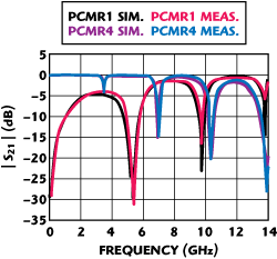
Figure 4 Measured and simulated results for the microstrip parallel-coupled resonator.
From the measurements, it is obvious that the assumed dielectric values are in error, with the error increasing at higher frequencies. To extract the correct dielectric constant and dielectric loss, these values are adjusted in ADS Momentum to match the frequency response until the predicted zero matches the measured zero. Figure 4 shows the fitted results for two PCMRs up to 14 GHz, after adjusting the dielectric parameters. In this case, the rise in these two parameters of DPC substrate is from 9.5 to 9.75 for the dielectric constant and 0.0004 to 0.002 for the dielectric loss, respectively. These values are more accurate than the assumed data at higher frequencies and can be widely used for substrate design and simulation.
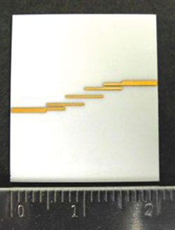
Figure 5 Photograph of the 10 GHz parallel-coupled line filter using DPC technology.
MICROWAVE CIRCUIT DESIGN
To validate the accuracy of extracted dielectric data, a microwave filter fabricated on a DPC substrate was demonstrated. This BPF, using a parallel-coupled line structure, has a center frequency of 10 GHz, a bandwidth of 15 percent, 0.1 dB equal-ripple response and third-order topology, and is shown in Figure 5. The BPF was designed and optimized with ADS Momentum using the extracted dielectric constant and dielectric loss. The TRL calibration kits were also fabricated on DPC substrates to cover the frequency range from 4 to 14 GHz.
With these test standards, the Anritsu test fixture’s coax-to-microstrip transitions and the microstrip lines up to the input and output ports of the filter can be de-embedded. The measured insertion loss and return loss are shown in Figure 6. Based on these experimental results, a good prediction of the filter response is achieved by using the extracted dielectric values in the EM simulator. The measured insertion loss of the BPF is only 0.5 dB at 10 GHz. It clearly demonstrated that the DPC process, fabricated with a ceramic substrate and copper conductor, provides excellent low-loss performance at high frequencies and offers the excellent ability to be used in RF packaging and microwave devices.
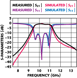
Figure 6 Measured and simulated characteristics of the 10 GHz DPC parallel-coupled line filter.
Conclusion
This article presents a DPC metallized substrate including the process flow, electrical properties extraction and a microwave circuit design. Owing to the use of the ceramic substrate and metallized copper conductor, the DPC substrate achieves good high-frequency electrical characteristics. Meanwhile, a simple extraction method to obtain the dielectric constant and dielectric loss for the DPC substrate was proposed, and a 10 GHz parallel-coupled line BPF with 0.5 dB insertion loss was built for further verification. This article clearly demonstrates that the DPC metallized substrate is quite suitable for RF and microwave package design, with its excellent low-loss performance.
References
1. M. Entezarian and R.A.L. Drew, “Direct Bonding of Copper to Aluminum Nitride,” Materials Science and Engineering, A-212, July 1996, pp. 206-212.
2. J. Schulz-Harder, “Advantages and New Development of Direct Boded Copper Substrates,” Microelectronics Reliability, Vol. 43, No. 3, 2003, pp. 359-365.
3. “DPC-Direct Plated Copper Thin Film Technology,” Tong Hsing, www.ready-sourcing.com/sourcing-news/electronic/dpc.html.
4. S.P. Ru, “Method for Removing Voids in a Ceramic Substrate,” US Patent, US 6,800,211 B2, October 2004.
5. M.K. Das, S.M. Voda and D.M. Pozar, “Two Methods for the Measurement of Substrate Dielectric Constant,” IEEE Transactions on Microwave Theory and Techniques, Vol. 35, No. 7, July 1987, pp. 636-642.
6. S.H. Chang, H. Kuan, H.W. Wu, R.Y. Yang and M.H. Weng, “Determination of Microwave Dielectric Constant by Two Microstrip Line Method Combined with EM Simulation,”Microwave and Optical Technology Letters, Vol. 48, No. 11, November 2006, pp. 2199-2121.
7. H. Yue, K.L. Virga and J.L. Prince, “Dielectric Constant and Loss Tangent Measurement Using a Stripline Fixture,” IEEE Transactions on Components, Packaging and Manufacturing Technology, Part B, Vol. 21, No. 4, November 1998, pp. 441-446.
8. P.A. Bernard and J.M. Gautray, “Measurement of Dielectric Constant Using a Microstrip Ring Resonator,” IEEE Transactions on Microwave Theory and Techniques, Vol. 39, No. 3, March 1991, pp. 592-595.
9. E.L. Holzman, “Wideband Measurement of the Dielectric Constant of an FR4 Substrate Using a Parallel-coupled Microstrip Resonator,” IEEE Transactions on Microwave Theory and Techniques, Vol. 54, No. 7, July 2006, pp. 3127-3130.
In the early 2000s, the chemical and physical properties of fullerenes were a hot topic in the field of research and development. Popular Science discussed possible uses of fullerenes (graphene) in armor.[41] In April 2003, fullerenes were under study for potential medicinal use: binding specific antibiotics to the structure to target resistant bacteria and even target certain cancer cells such as melanoma. The October 2005 issue of Chemistry & Biology contained an article describing the use of fullerenes as light-activated antimicrobial agents.[42]
In the field of nanotechnology, heat resistance and superconductivity are some of the more heavily studied properties.
A common method used to produce fullerenes is to send a large current between two nearby graphite electrodes in an inert atmosphere. The resulting carbon plasma arc between the electrodes cools into sooty residue from which many fullerenes can be isolated.
There are many calculations that have been done using ab-initio quantum methods applied to fullerenes. By DFT and TD-DFT methods one can obtain IR, Raman and UV spectra. Results of such calculations can be compared with experimental results.
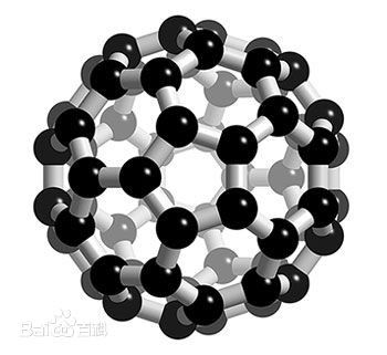
Researchers have been able to increase the reactivity of fullerenes by attaching active groups to their surfaces. Buckminsterfullerene does not exhibit “superaromaticity“: that is, the electrons in the hexagonal rings do not delocalize over the whole molecule.
A spherical fullerene of n carbon atoms has n pi-bonding electrons, free to delocalize. These should try to delocalize over the whole molecule. The quantum mechanics of such an arrangement should be like one shell only of the well-known quantum mechanical structure of a single atom, with a stable filled shell for n = 2, 8, 18, 32, 50, 72, 98, 128, etc.; i.e. twice a perfect square number; but this series does not include 60. This 2(N + 1)2 rule (with N integer) for spherical aromaticity is the three-dimensional analogue of Hückel’s rule. The 10+ cation would satisfy this rule, and should be aromatic. This has been shown to be the case using quantum chemical modelling, which showed the existence of strong diamagnetic sphere currents in the cation.[43]
As a result, C60 in water tends to pick up two more electrons and become an anion. The nC60 described below may be the result of C60 trying to form a loose metallic bond.
Fullerenes are stable, but not totally unreactive. The sp2-hybridized carbon atoms, which are at their energy minimum in planar graphite, must be bent to form the closed sphere or tube, which produces angle strain. The characteristic reaction of fullerenes is electrophilic addition at 6,6-double bonds, which reduces angle strain by changing sp2-hybridized carbons into sp3-hybridized ones. The change in hybridized orbitals causes the bond angles to decrease from about 120° in the sp2 orbitals to about 109.5° in the sp3 orbitals. This decrease in bond angles allows for the bonds to bend less when closing the sphere or tube, and thus, the molecule becomes more stable.
Other atoms can be trapped inside fullerenes to form inclusion compounds known as endohedral fullerenes. An unusual example is the egg-shaped fullerene Tb3N@C84, which violates the isolated pentagon rule.[44] Recent evidence for a meteor impact at the end of the Permian period was found by analyzing noble gases so preserved.[45] Metallofullerene-based inoculates using the rhonditic steel process are beginning production as one of the first commercially viable uses of buckyballs.
Fullerene production processes comprise the following five subprocesses: (i) synthesis of fullerenes or fullerene-containing soot; (ii) extraction; (iii) separation (purification) for each fullerene molecule, yielding pure fullerenes such as C60; (iv) synthesis of derivatives (mostly using the techniques of organic synthesis); (v) other post-processing such as dispersion into a matrix. The two synthesis methods used in practice are the arc method, and the combustion method. The latter, discovered at the Massachusetts Institute of Technology, is preferred for large scale industrial production.[57][58]
Fullerenes have been extensively used for several biomedical applications including the design of high-performance MRI contrast agents, X-ray imaging contrast agents, photodynamic therapy and drug and gene delivery, summarized in several comprehensive reviews.
Royal Technology and “School of Material Science & Engineering Shanghai University” has been coopereting together to develope the PVD coating machine for more applications R & D. With inductive evaporation method to deposit thin film in high vacuum environment on products.